@anernest
Ensure that the LCD is an EDP interface and the touch is an IIC interface. In principle, it can light up normally, but the driver part needs to be modified. Check if there are any universal specifications later.
Group Details Private
Global Moderators
Forum wide moderators
-
RE: DIY Tabletposted in Peripheral
-
Deploying Deepseek R7 model on coolpiposted in AI Algorithm
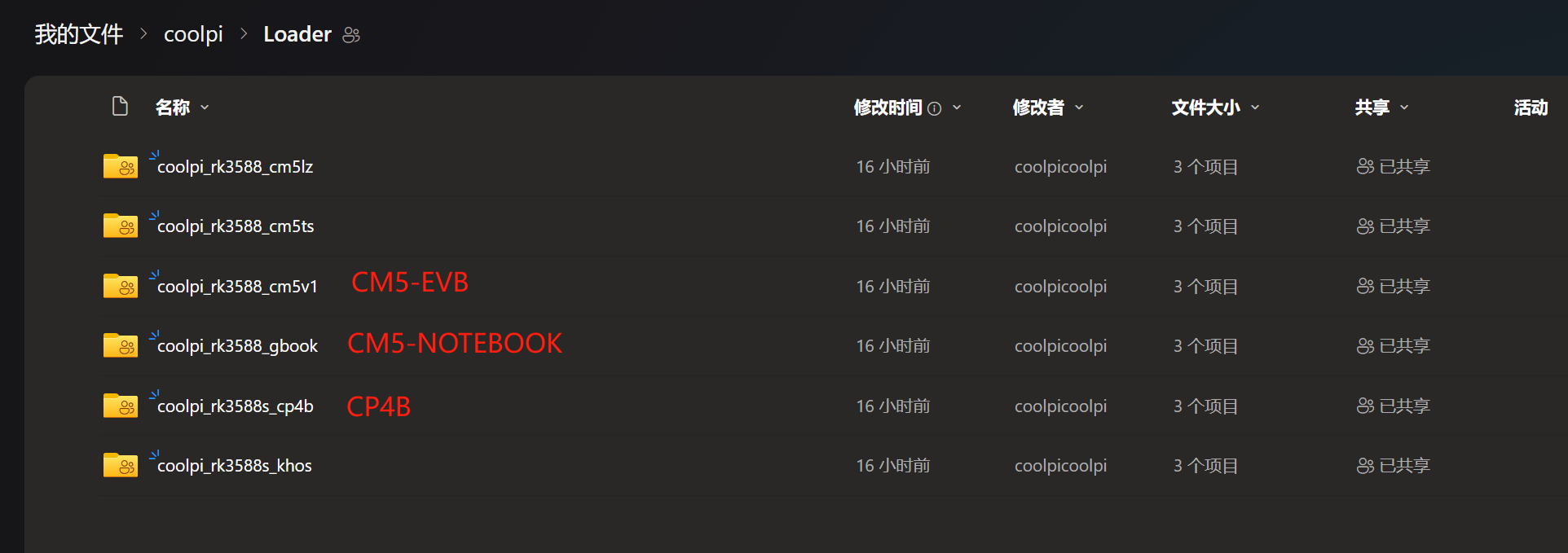
The R7 model is suitable for cp4b (16G) cm5-evb (32G) cm5-notebook (32G) machines, and low memory capacity machines are only suitable for the R1.5 model. The operating system defaults to Ubuntu 24.04.
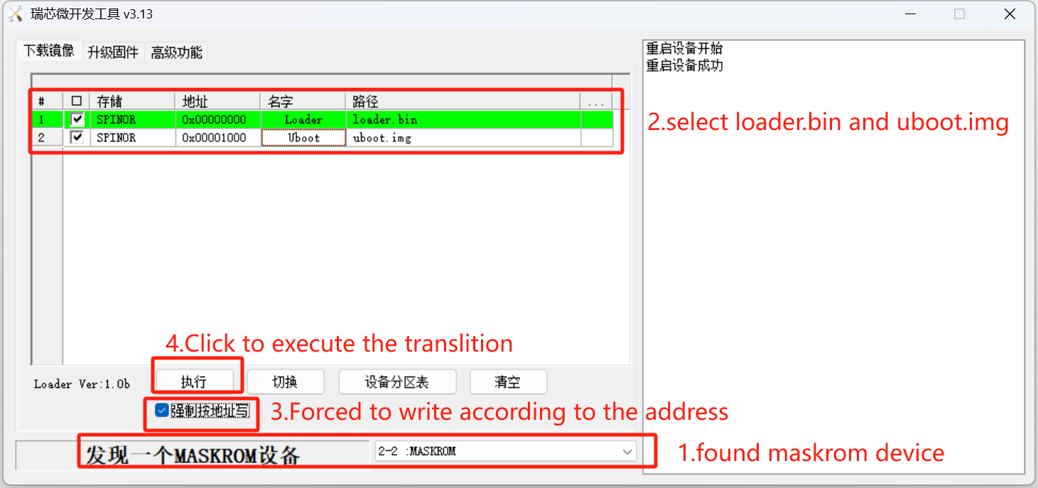
- Update the system loader to the latest version
Download the latest loader file from Baidu Netdisk or OneDrive
The machine enters Maskrom and then upgrades the loader according to the configuration shown in the following figure.
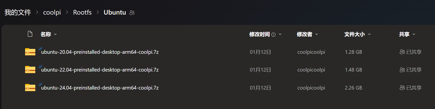
- Upgrade to the latest Ubuntu 24.04 image
Download the latest Ubuntu 24.04 image from Baidu Netdisk or OneDrive and upgrade. Currently, CP4B/CM5-EVB/CM5-Notebook uses a unified image file.
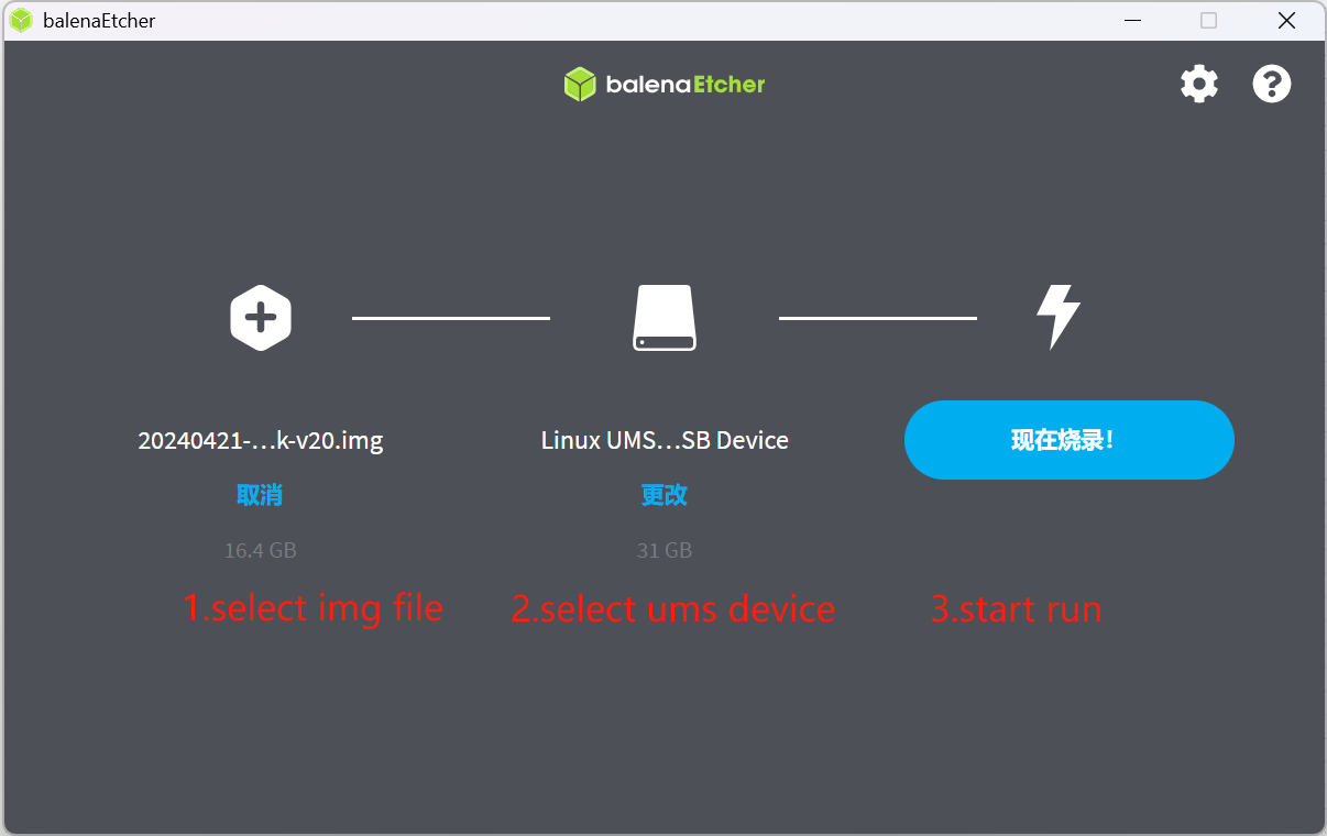
The machine enters UMS mode (run the command "sudo reboot UMS" in a shell window or press the power button multiple times after booting), and upgrade using Etcher.
Attention: The downloaded image needs to be decompressed before it can be used.
- Download Model
Obtain the converted rknn model from the following website. Deepseek can choose the 1.5b/7b model. Of course, if you are interested, you can convert it yourself. Tools and documentation will be provided later.
https://huggingface.co/c01zaut
- Synchronize RKLMM project
git clone https://github.com/coolpi-george/rknn-llm.git
cd rknn-llm/examples/DeepSeek-R1-Distill-Qwen-1.5B_Demo/deploy/
./build-linux.sh
Compiled successfully as shown in the following figure
tmjs@tmjs:~/share/coolpi-george/rknn-llm/examples/DeepSeek-R1-Distill-Qwen-1.5B_Demo/deploy$ ./build-linux.sh
-- Configuring done (0.0s)
-- Generating done (0.0s)
-- Build files have been written to: /home/tmjs/share/coolpi-george/rknn-llm/examples/DeepSeek-R1-Distill-Qwen-1.5B_Demo/deploy/build/build_linux_aarch64_Release
[100%] Built target llm_demo
[100%] Built target llm_demo
Install the project...
-- Install configuration: "Release"
-- Up-to-date: /home/tmjs/share/coolpi-george/rknn-llm/examples/DeepSeek-R1-Distill-Qwen-1.5B_Demo/deploy/install/demo_Linux_aarch64/./llm_demo
-- Up-to-date: /home/tmjs/share/coolpi-george/rknn-llm/examples/DeepSeek-R1-Distill-Qwen-1.5B_Demo/deploy/install/demo_Linux_aarch64/lib/librkllmrt.so
sudo cp install/demo_Linux_aarch64/lib/librkllmrt.so /usr/lib/aarch64-linux-gnu/- Load the model and run it
tmjs@tmjs:~/share/coolpi-george/rknn-llm/examples/DeepSeek-R1-Distill-Qwen-1.5B_Demo/deploy/install/demo_Linux_aarch64$ ./llm_demo /home/tmjs/share/DeepSeek-R1-Distill-Qwen-1.5B_RKLLM/deepseek-r1-1.5B-rkllm1.1.4.rkllm 100000 100000 rkllm init start I rkllm: rkllm-runtime version: 1.1.4, rknpu driver version: 0.9.7, platform: RK3588 rkllm init success **********************可输入以下问题对应序号获取回答/或自定义输入******************** [0] 现有一笼子,里面有鸡和兔子若干只,数一数,共有头14个,腿38条,求鸡和兔子各有多少只? [1] 有28位小朋友排成一行,从左边开始数第10位是学豆,从右边开始数他是第几位? ************************************************************************* user: 你好 robot: <think> </think> 你好!很高兴见到你,有什么我可以帮忙的吗?无论是学习、工作还是生活中的问题,都可以告诉我哦! user: 帮我写一首赞美春天的歌曲 robot: <think> 嗯,用户让我帮他写一首赞美春天的歌曲。首先,我得考虑用户的需求是什么。他可能是个学生,老师布置了这样的作业,或者他自己想表达对春天的喜爱。也有可能是喜欢音乐创作的人,想要一首有诗意、充满生机的作品。 接下来,我要分析用户可能没有明确说出来的深层需求。也许他希望这首诗不仅要有春天的意象,还要有情感上的共鸣,比如对自然美景的赞美,或者是对未来的美好期许。另外,用户可能还希望这首诗能够传达一种宁静而美好的氛围,适合在春天的早晨或午后听。 然后,我得考虑如何将春天的元素融入到歌曲里。春天通常与花开、绿草、鸟鸣、风声等相关联。这些元素可以用来营造出春天的氛围,同时让歌曲有节奏感和韵律感。比如,用轻快的鼓点来表现风的声音,或者用轻柔的旋律来描绘花开的美丽。 我还得考虑诗的结构和押韵方式。可能采用四句一节,每句七个字,这样比较符合中文诗歌的韵律。同时,每一句都要有独特的意象,避免重复,让整首诗更有层次感。 另外,用户可能希望这首诗不仅仅是描述春天,还能传达一种积极向上的情绪。因此,在用词和节奏上要显得温暖而充满希望。比如,使用一些积极向上的词汇,如“绿”、“欢”、“暖”等,来增强整体的感染力。 最后,我需要确保整首诗流畅自然,情感真挚。可能还需要加入一些比喻或拟人手法,让春天的景象更加生动形象。例如,把花朵比作小舞者,或者把风的声音比作春天的旋律。 总结一下,用户的需求是写一首赞美春天的歌曲,我需要结合春天的元素,使用富有节奏感和韵律的结构,传达出宁静而美好的氛围,并且情感真挚。这样既满足了用户的创作需求,也能让这首诗打动人心。 </think> ## 《春日》 花儿在枝头摇曳 轻盈的裙摆上 藏着春天的旋律 风儿轻轻吹过 带来泥土的气息 我听见了花开的声音 在耳畔流淌 每一朵花都是我的家 它们是春天的歌谣 在记忆里 等待着 我听见了 春天的节奏 在心上 它是一首永不停歇的诗 - Update the system loader to the latest version
-
RE: DIY Tabletposted in Peripheral
@anernest
These features are already supported on laptop products. -
RE: DIY Tabletposted in Peripheral
We are looking forward to your work and can provide technical support.
Thank you! -
RE: Cool Pi ARM Notebook Previewposted in News
@Chan
如下链接可以购买:
https://item.taobao.com/item.htm?id=769972910823&ns=1&pisk=geXbTQxh5q0b5baGZZqyR5x3Bvv65uyElctOxGHqXKpvW_sh5ErgiK5W5aQWkxr0iCL1oKdGgF825dsGRuzULJScmdv88yyFYmcgnpcxDn3w24K6CnebU7rAmdvT80kTTJscJJMnfrx92utwbn3OWhL8eUxwWfQ9kQ3JAHv9BrL2wl1OCGRDHKdyBG8lnq4xMha58HcV7KY9qzsdjslMsrKTanxvgE8mnFHkrhGx6IHtwLKDAmptHhe8eHKZDnptBQLJrhp9WNpTVLh754taGhIbcP7ev0Me4iLSBABYIITBvfksCsxvGOIvPgSPFnOXRQ7OETXAzGBVnQV-NdjPON1OJzl2k6tCPB5bRx_CohI6XZwnAUBffTOcaDDOVCTfwtdSXAIXEFdd1ZajiECVPBxJwcwH4w8RmtC7j4IA8E9v2QyLAgdOatAh3zHXp6j231QLzj8AOhIrsv8QMjhsVBD6Ver7Vfcif-ByL_w0G6RvqneUVugSsIKkVer7VfcMM3xATuZSPff..&priceTId=2147864117368238436881813eaab5&skuId=5340285281741&spm=a21n57.1.hoverItem.1&utparam={"aplus_abtest"%3A"3a39d1f4fb9e1d7bf8927ec6e59f0413"}&xxc=ad_ztc -
RE: CoolPi 4B OV5647 摄像头图片全黑posted in Pi 4B
@traceback
使用QV4L2测试一下节点,确实是否可以正常获取图像,除了型号以外,不同的sensor镜头也会对图像产生影响。 -
RE: Tried to update the boot loaderposted in PI CM5 Laptop
@Momo-0
This firmware is fine, you can try again a few times. If it still doesn't work, follow the following steps:
1.Remove the back cover of the machine. There is a button on the motherboard near the SSD connector。
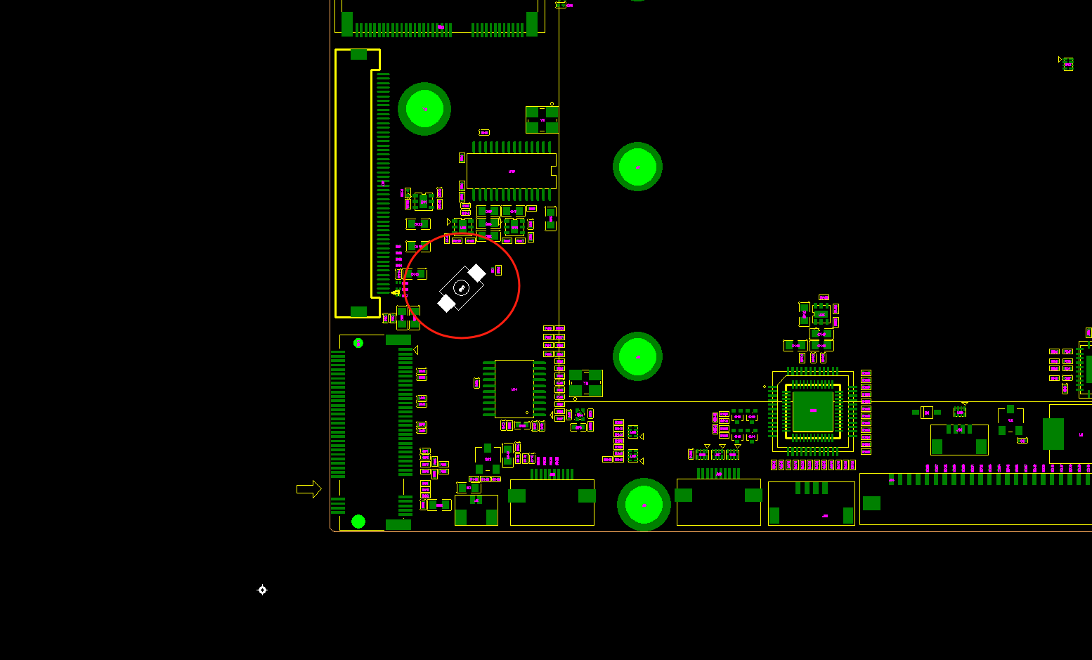
2.Press the button, then press the power button on the laptop to turn it on, and the machine will enter maskrom mode.
3.Burn in the firmware again using the previous method. -
RE: Cool Pi Cm5-Laptop Linux Quick Start Guideposted in PI CM5 Laptop
@Momo-0
Usually caused by incorrect recognition of file system partitions, pay attention to checking the cmdline. -
RE: Tried to update the boot loaderposted in PI CM5 Laptop
@Momo-0
Upgrade the loader using the attachment compressed file as shown in the following figure.
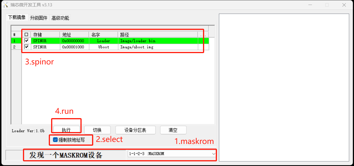
RKDevTool_v3.13_for_window_1.17.113.rar